
成功的纳法Alex
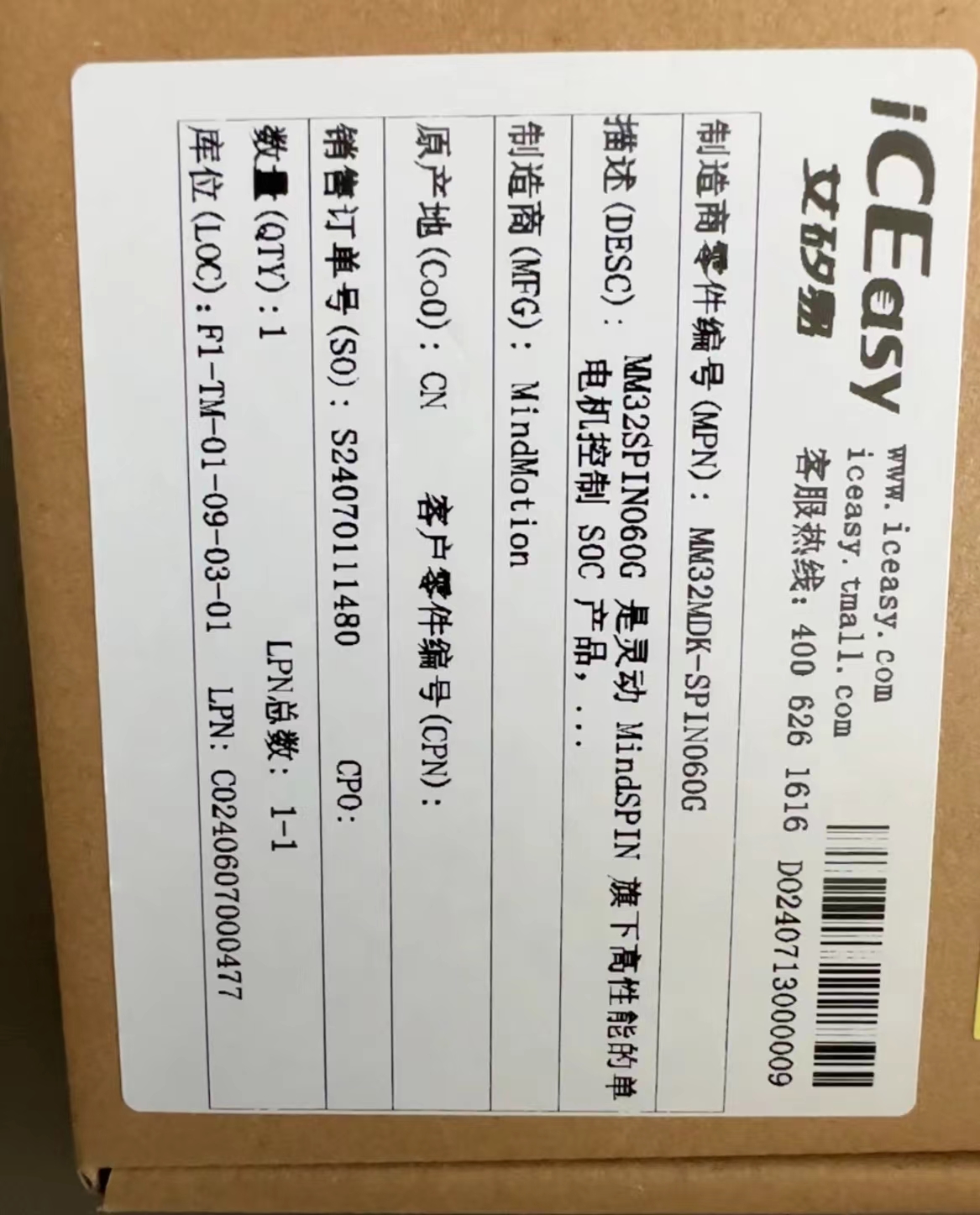
关于ICEASY商城申请-灵动MM32SPIN060G的测评
一、MM32SPIN060G简介
使用高性能的 Arm® Cortex-M0 为内核的 32 位微控制器,最高工作频率可达 48MHz,内置高速存储器,丰富的 I/O 端口和多种外设。
- 16KB Flash,2KB SRAM
- 包含 12 位的 ADC,采样速度高达 1 Msps
- 2 个通用定时器、1 个针对电机控制的 PWM 高级定时器
- 1 个 I2C 接口、 2 个 UART 接口
- 针对电机应用内置 2 个运放
- 预驱工作电压高达 36V
- 工作温度范围(环境温度)-40℃ - 105℃
- 提供 TSSOP28,QFN28 封装
二、简单开箱+介绍
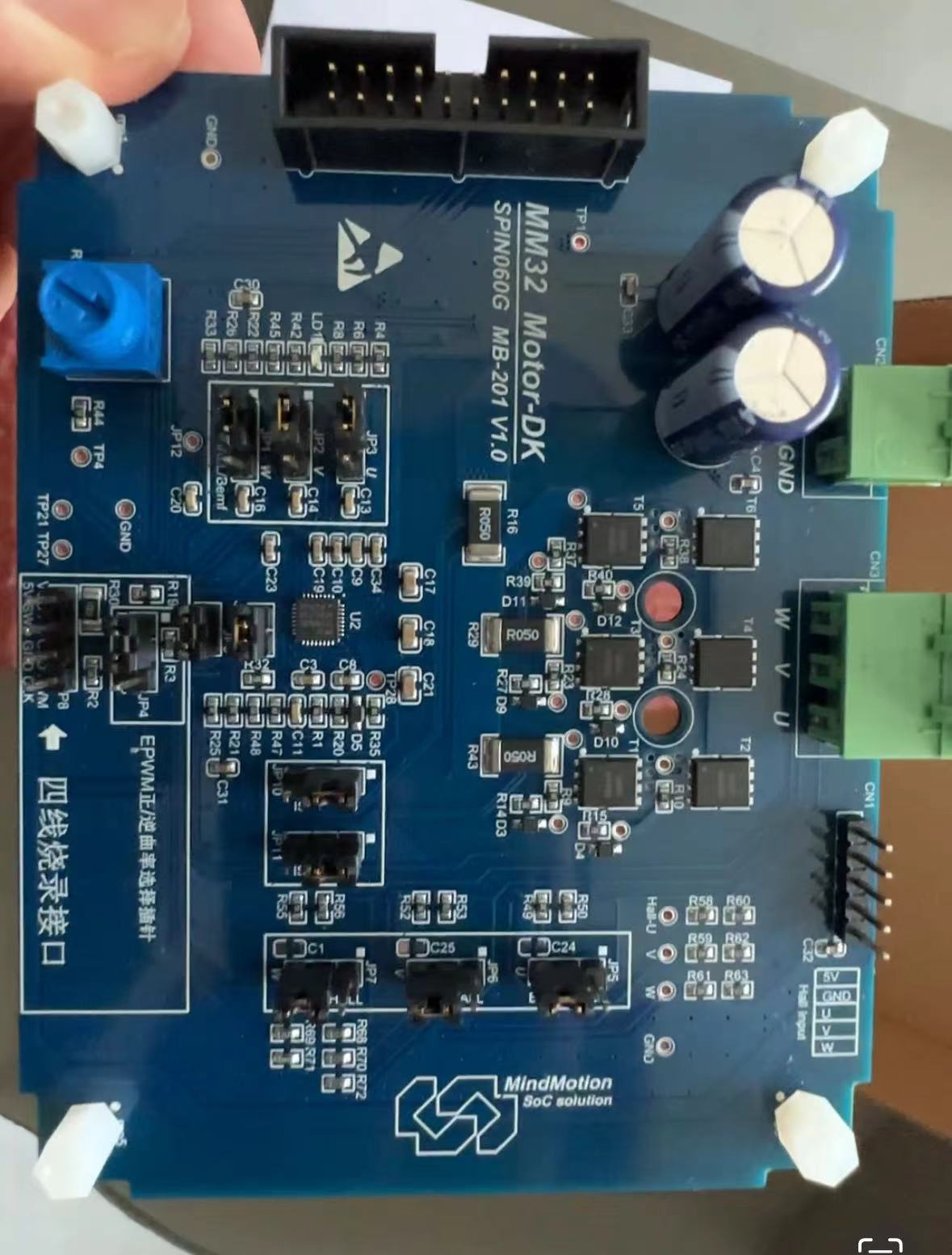
板子硬件上包含有
1.直流电源输入,其范围在5.5~18V
2.UVW三相电压
3.霍尔接口
4.电位器
5.烧录调试接口
6.反电动势或者霍尔跳线接口
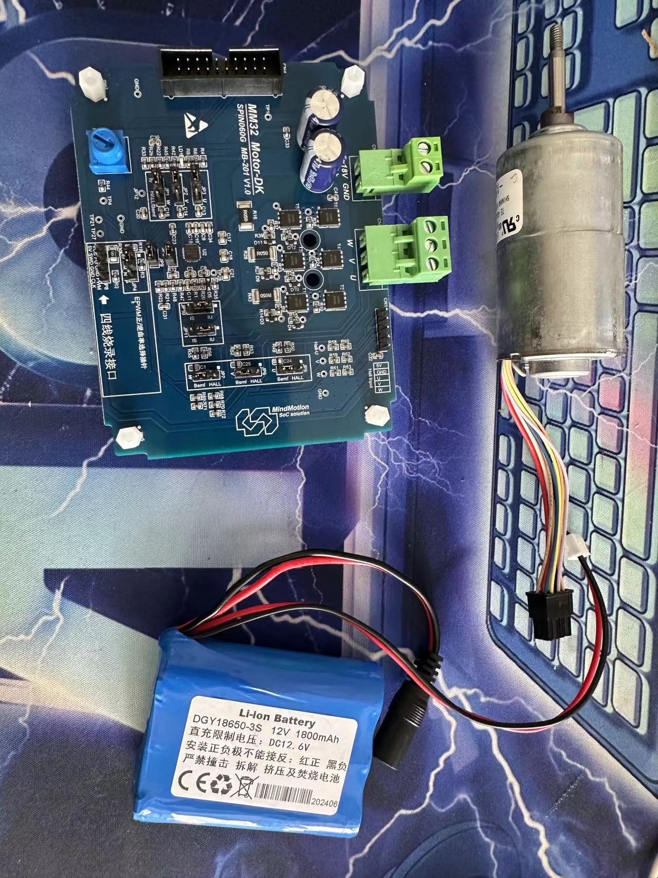
三、测评所用到的硬件
MM32SPIN060G、12V电源、无刷电机(DC105)
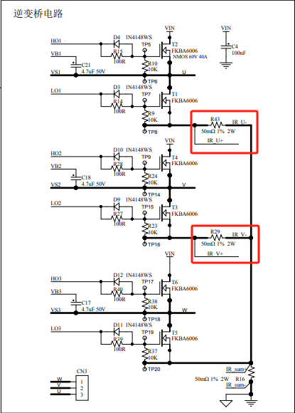
四、双电阻采样-无感FOC
1.双电阻采样电路,选择插针,采集U相、V相电流,通过三项电流之和为零的原理计算出W相电流。

2.无位置传感器控制
通过矢量控制的介绍可知转子位置信息对矢量控制至关重要,PMSM 的转子位 置信息可以通过专用的位置传感器,例如光电编码器、磁编码器、测速发电机或 者开关霍尔等传感器获取。速度传感器会给电机带来额外的硬件成本和维护成本, 因此近些年无位置传感器控制应用越来越广泛。目前主流的无位置传感器算法包 括滑模观测器、反电势观测器、磁链观测器、卡尔曼滤波器、模型参考自适应观 测器等算法,本应用使用了滑模观测器法来实时观测转子位置。 滑模控制应用于转子位置估算中位置较准确,对控制对象的参数变化及扰动具有 自适应能力,而且该方案实现简单,对 MCU 资源没有太大要求。
五、官方代码大致介绍
ADC采样 ,通过定时器触发方式,
void Bsp_Adc_Init(void)
{
GPIO_InitTypeDef GPIO_InitStructure;
GPIO_StructInit(&GPIO_InitStructure);
/* ADC Clock Enable */
RCC_AHBPeriphClockCmd(ADC_GPIO_CLK, ENABLE);
/*Condiv ADC pin */
GPIO_InitStructure.GPIO_Mode = GPIO_Mode_AIN;
GPIO_InitStructure.GPIO_Pin = VR_PIN;//调速
GPIO_Init(VR_PORT, &GPIO_InitStructure);
GPIO_InitStructure.GPIO_Pin = VBUS_PIN;//电压
GPIO_Init(VBUS_PORT, &GPIO_InitStructure);
GPIO_InitStructure.GPIO_Pin = IR_V_PIN;//V相电流
GPIO_Init(IR_V_PORT, &GPIO_InitStructure);
GPIO_InitStructure.GPIO_Pin = IR_U_PIN;//U相电流
GPIO_Init(IR_U_PORT, &GPIO_InitStructure);
}
void Board_ADC_Init(void)
{
/*ADC RANK Array*/
ADC_Channel_TypeDef sUserAdc1Channel[4];
/* Condiv the ADC RANK Sequence*/
sUserAdc1Channel[0].u8Rank = IR_U_RANK;
sUserAdc1Channel[0].sAdcChannel = IR_U_CHANNEL;
sUserAdc1Channel[0].pNext = &sUserAdc1Channel[1];
sUserAdc1Channel[1].u8Rank = IR_V_RANK;
sUserAdc1Channel[1].sAdcChannel = IR_V_CHANNEL;
sUserAdc1Channel[1].pNext = &sUserAdc1Channel[2];
sUserAdc1Channel[2].u8Rank = VBUS_RANK;
sUserAdc1Channel[2].sAdcChannel = VBUS_CHANNEL;
sUserAdc1Channel[2].pNext = &sUserAdc1Channel[3];
sUserAdc1Channel[3].u8Rank = VR_RANK;
sUserAdc1Channel[3].sAdcChannel = VR_CHANNEL;
sUserAdc1Channel[3].pNext = NULL;
/* Select the ADC external trigger source of the ADC is T1_CC4*/
Drv_Adc_Basic_Init(ADC1, ADC_ExtTrig_T1_CC4);
/* Select the ADC sample time*/
Drv_Adc_Channel_Init(ADC1, sUserAdc1Channel, ADC_SampleTime_2_5);
}
比较器
void Bsp_Comp_Init(void)
{
GPIO_InitTypeDef GPIO_InitStructure;
GPIO_StructInit(&GPIO_InitStructure);
/* COMP Clock Enable */
RCC_AHBPeriphClockCmd((COMP_GPIO_CLK), ENABLE);
GPIO_InitStructure.GPIO_Pin = COMP_INP_PIN;
GPIO_InitStructure.GPIO_Mode = GPIO_Mode_AIN;
GPIO_InitStructure.GPIO_Speed = GPIO_Speed_High;
GPIO_Init(COMP_INP_PORT, &GPIO_InitStructure);
}
void Board_Comp_Init(void)
{
COMP_Input_TypeDef sUserCompInput;
/* Select the inverting input of the comparator */
sUserCompInput.sCompInvertingInput = COMP_INVERTING;
/* Select the non inverting input of the comparator*/
sUserCompInput.sCompNonInvertingInput = COMP_NON_INVERTING;
/* Select comparator external reference voltage */
sUserCompInput.u8CompCrvSelect = COMP_CRV_VOLTAGE_SELECT;
/* Initializes the COMP according to the specified parameters in the COMP_Input_TypeDef */
Drv_Comp_Init(COMP_NUMBER,&sUserCompInput);
}
六路PWM初始化
void Bsp_Pwm_Init(void)
{
GPIO_InitTypeDef GPIO_InitStructure;
GPIO_StructInit(&GPIO_InitStructure);
/* PWM Clock Enable */
RCC_AHBPeriphClockCmd(BLDC1_GPIO_CLK, ENABLE);
/*Condiv GPIO pin : PWM_Pin */
GPIO_InitStructure.GPIO_Pin = BLDC1_UH_PIN;
GPIO_InitStructure.GPIO_Speed = GPIO_Speed_High;
GPIO_InitStructure.GPIO_Mode = GPIO_Mode_AF_PP;
GPIO_Init(BLDC1_UH_PORT, &GPIO_InitStructure);
GPIO_InitStructure.GPIO_Pin = BLDC1_VH_PIN;
GPIO_Init(BLDC1_VH_PORT, &GPIO_InitStructure);
GPIO_InitStructure.GPIO_Pin = BLDC1_WH_PIN;
GPIO_Init(BLDC1_WH_PORT, &GPIO_InitStructure);
GPIO_InitStructure.GPIO_Pin = BLDC1_UL_PIN;
GPIO_Init(BLDC1_UL_PORT, &GPIO_InitStructure);
GPIO_InitStructure.GPIO_Pin = BLDC1_VL_PIN;
GPIO_Init(BLDC1_VL_PORT, &GPIO_InitStructure);
GPIO_InitStructure.GPIO_Pin = BLDC1_WL_PIN;
GPIO_Init(BLDC1_WL_PORT, &GPIO_InitStructure);
/*selects the pin to used as Alternate function of PWM*/
/*六个IO口,六个桥臂 UVW三个上桥 UVW三个下桥*/
GPIO_PinAFConfig(BLDC1_UH_PORT, BLDC1_UH_PIN_SRC, BLDC1_UH_PIN_AF);
GPIO_PinAFConfig(BLDC1_VH_PORT, BLDC1_VH_PIN_SRC, BLDC1_VH_PIN_AF);
GPIO_PinAFConfig(BLDC1_WH_PORT, BLDC1_WH_PIN_SRC, BLDC1_WH_PIN_AF);
GPIO_PinAFConfig(BLDC1_UL_PORT, BLDC1_UL_PIN_SRC, BLDC1_UL_PIN_AF);
GPIO_PinAFConfig(BLDC1_VL_PORT, BLDC1_VL_PIN_SRC, BLDC1_VL_PIN_AF);
GPIO_PinAFConfig(BLDC1_WL_PORT, BLDC1_WL_PIN_SRC, BLDC1_WL_PIN_AF);
GPIO_InitStructure.GPIO_Pin = GPIO_Pin_3;
GPIO_InitStructure.GPIO_Speed = GPIO_Speed_High;
GPIO_InitStructure.GPIO_Mode = GPIO_Mode_Out_PP;
GPIO_Init(GPIOB, &GPIO_InitStructure);
GPIO_SetBits(GPIOB, GPIO_Pin_3);
}
void Drv_Pwm_Init(TIM_TypeDef * pTim, uint16_t u16Period,uint16_t u16DeadTime)
{
/** Define the struct of the PWM configuration */
TIM_TimeBaseInitTypeDef TIM_TimeBaseStructure;
TIM_BDTRInitTypeDef TIM_BDTRInitStruct;
TIM_OCInitTypeDef TIM_OCInitStructure;
/** Enable the TIM1 clock */
RCC_APB1PeriphClockCmd(RCC_APB1ENR_TIM1_Msk, ENABLE);
/**
* Sets the value of the automatic reload register Period for the next update event load activity
* Set the Prescaler value used as the divisor of the TIMx clock frequency
* Set clock split :TDTS = TIM_CKD_DIV1
* TIM center aligned mode1
*/
TIM_TimeBaseStructure.TIM_Period = u16Period;
TIM_TimeBaseStructure.TIM_Prescaler = 0;
TIM_TimeBaseStructure.TIM_ClockDivision = 0;
TIM_TimeBaseStructure.TIM_CounterMode = TIM_CounterMode_CenterAligned2;
TIM_TimeBaseStructure.TIM_RepetitionCounter = 0;
TIM_TimeBaseInit(pTim, &TIM_TimeBaseStructure);
/**
* Enable state selection in running mode
* Enable state selection in idle mode
* Software error lock configuration: lock closed without protection
* DTG[7:0] dead zone generator configuration (dead zone time DT)
*/
/**
* TDTS = 125nS(8MHz)
* DTG[7: 5] = 0xx => DT = DTG[7: 0] * Tdtg, Tdtg = TDTS;
* DTG[7: 5] = 10x => DT =(64+DTG[5: 0]) * Tdtg, Tdtg = 2 * TDTS;
* DTG[7: 5] = 110 => DT =(32+DTG[4: 0]) * Tdtg, Tdtg = 8 * TDTS;
* DTG[7: 5] = 111=> DT =(32 + DTG[4: 0]) * Tdtg, Tdtg = 16 * TDTS;
*/
TIM_BDTRInitStruct.TIM_OSSRState = TIM_OSSRState_Enable;
TIM_BDTRInitStruct.TIM_OSSIState = TIM_OSSIState_Enable;
TIM_BDTRInitStruct.TIM_LOCKLevel = TIM_LOCKLevel_OFF;
TIM_BDTRInitStruct.TIM_DeadTime = u16DeadTime;
/**
* Brake configuration: enable brake
* Brake input polarity: active in low level
* Auto output enable configuration: Disable MOE bit hardware control
*/
TIM_BDTRInitStruct.TIM_Break = TIM_Break_Enable;
TIM_BDTRInitStruct.TIM_BreakPolarity = TIM_BreakPolarity_High;
TIM_BDTRInitStruct.TIM_AutomaticOutput = TIM_AutomaticOutput_Disable;
TIM_BDTRConfig(pTim, &TIM_BDTRInitStruct);
TIM_BreakInputFilterConfig(pTim,TIM_COMPBKIN_COMP2,TIM_BKINF_2);
TIM_BreakInputFilterCmd(pTim, ENABLE);
/**
* Mode configuration: PWM mode 1
* Output status setting: enabl0Ce output
* Complementary channel output status setting: enable output
* Sets the pulse value to be loaded into the capture comparison register
* Output polarity is high
* N Output polarity is high
*/
TIM_OCInitStructure.TIM_OCMode = TIM_OCMode_PWM2;
TIM_OCInitStructure.TIM_OutputState = TIM_OutputState_Enable;
TIM_OCInitStructure.TIM_OutputNState = TIM_OutputNState_Enable;
TIM_OCInitStructure.TIM_Pulse = 0;
TIM_OCInitStructure.TIM_OCPolarity = TIM_OCPolarity_High;
TIM_OCInitStructure.TIM_OCNPolarity = TIM_OCNPolarity_High;
TIM_OCInitStructure.TIM_OCIdleState = TIM_OCIdleState_Reset;
TIM_OCInitStructure.TIM_OCNIdleState = TIM_OCNIdleState_Reset;
TIM_OC1Init(pTim, &TIM_OCInitStructure);
TIM_OC2Init(pTim, &TIM_OCInitStructure);
TIM_OC3Init(pTim, &TIM_OCInitStructure);
/** Initialize the CCR4 trigger point */
TIM_OCInitStructure.TIM_Pulse = 10;
TIM_OCInitStructure.TIM_OutputState = TIM_OutputState_Disable;
TIM_OCInitStructure.TIM_OutputNState = TIM_OutputNState_Disable;
TIM_OC4Init(pTim, &TIM_OCInitStructure);
/** Enable CH1, 2, and 3 to be preloaded */
TIM_OC1PreloadConfig(pTim, TIM_OCPreload_Enable);
TIM_OC2PreloadConfig(pTim, TIM_OCPreload_Enable);
TIM_OC3PreloadConfig(pTim, TIM_OCPreload_Enable);
/** Enable TIMx's preloaded register on ARR */
TIM_ARRPreloadConfig(pTim, ENABLE);
/** Enable the TIM1 */
TIM_Cmd(pTim, ENABLE);
/** Main Output Enable:Disable the MOE bit */
TIM_CtrlPWMOutputs(pTim, DISABLE);
}
运算放大器初始化
void Bsp_Op_Init(void)
{
GPIO_InitTypeDef GPIO_InitStructure;
GPIO_StructInit(&GPIO_InitStructure);
/* GPIO Ports Clock Enable */
RCC_AHBPeriphClockCmd(OPAMP_GPIO_CLK, ENABLE);
/*Condiv GPIO pin : OPAMP1_Pin */
GPIO_InitStructure.GPIO_Mode = GPIO_Mode_AIN;
GPIO_InitStructure.GPIO_Pin = OPAMP1_INM_PIN;
GPIO_Init(OPAMP1_INM_PORT, &GPIO_InitStructure);
GPIO_InitStructure.GPIO_Pin = OPAMP1_INP_PIN;
GPIO_InitStructure.GPIO_Mode = GPIO_Mode_AIN;
GPIO_Init(OPAMP1_INP_PORT, &GPIO_InitStructure);
/*Condiv GPIO pin : OPAMP2_Pin */
GPIO_InitStructure.GPIO_Mode = GPIO_Mode_AIN;
GPIO_InitStructure.GPIO_Pin = OPAMP2_INM_PIN;
GPIO_Init(OPAMP2_INM_PORT, &GPIO_InitStructure);
GPIO_InitStructure.GPIO_Pin = OPAMP2_INP_PIN;
GPIO_InitStructure.GPIO_Mode = GPIO_Mode_AIN;
GPIO_Init(OPAMP2_INP_PORT, &GPIO_InitStructure);
}
void Board_Opamp_Init(void)
{
/* op-amp Clock Enable */
RCC_APB1PeriphClockCmd(RCC_APB1ENR_OPA1_Msk, ENABLE);
RCC_APB1PeriphClockCmd(RCC_APB1ENR_OPA2_Msk, ENABLE);
/*Enable the specified OPAMP peripheral*/
OPAMP_Cmd(OPAMP1,ENABLE);
OPAMP_Cmd(OPAMP2,ENABLE);
}
主函数
int main(void)
{
/* Condiv the system clock */
Systick_Init(SystemCoreClock / 1000);
Systick_Delay(200);
/* 初始化电机控制参数 */
Init_Parameter(&Motor_1st);
/* 初始化所有GPIO */
Bsp_Gpio_Init();
/* 初始化所有已配置的外围设备 */
Peripheral_Init();
/* 初始化中断*/
Interrupt_Init();
while(1)
{
/*IWDG_ReloadCounter*/
IWDG_RELOAD_COUNT();
if(Motor_1st.USER.bSlowLoopFlag)
{
/* Slow Loop Statemachine */
s_STATE_SLOW[eM1_MainState]();
Motor_1st.USER.bSlowLoopFlag = 0;
}
}
}
这里看门狗防止系统出现问题跑飞,下面的if是通过状态机进行电机的控制。
大致解释一下,状态机的执行过程。首先Motor_1st.USER.bSlowLoopFlag 为真(此历程提供了低速循环和高速循环,这里使用的是低速循环),则通过 s_STATE_SLOW[eM1_MainState]() 调用执行当前状态对应的函数。其中s_STATE_SLOW 是一个包含四个函数指针的数组,这些函数指针分别指向 M1_Fault_Slow、M1_Init_Slow、M1_Stop_Slow 和 M1_Run_Slow 四个函数。eM1_MainState 是一个枚举变量( MainState_Fault = 0, MainState_Init = 1,MainState_Stop = 2, MainState_Run = 3,),它决定了从 s_STATE_SLOW 数组中选择哪个函数指针进行调用。进而完成电机的启动过程。
六、事物演示
工程附件
MM32SPIN060G_FOC_2R_V_1.34.zip
版块:
单片机/MCU论坛
2024/08/08 23:01


全部评论